Design of a dedicated edge detection processor: hardware implementation of a Sobel filter⚓
Important links
- VHDL Syntax: VHDL Quick Ref
- Markdown Syntax: Markdown Syntax Introduction
Introduction⚓
In this series of practical work sessions, we are interested in the design of a hardware architecture to accelerate the performance of edge detection in terms of execution time.
An incomplete proposal of such an architecture was introduced in the course (figure below) with two main components:
- An operative unit that integrates registers and functional units (arithmetic and logic operators).
- A control unit that integrates a Finite State Machine (FSM) and an address generator.

In addition to the components that make up the core of the processor, the complete edge detection system includes interfaces and input/output memories, including a VGA screen display controller.
Thus, the objective of this series of three practical work sessions (in project mode) is to develop and implement this hardware acceleration solution. The different steps of the associated design flow will be illustrated: (a) modeling and development of the different components of this hardware solution, (b) logic synthesis, integration and prototyping on FPGA board, (c) implementation of integration test, characterization and performance validation.
The project must end with a performance analysis phase.
The hardware platform that will be used for prototyping is based on the Digilent Nexys 4 board represented in figur below and includes an Xilinx Artix 7 FPGA (reference XC7A100T-CSG324) and many peripherals and interfaces including a VGA output.

The development environment associated with this board will be the Xilinx Vivado design suite.
Regarding the sizing of the architecture, simulations and experiments on the board, we will consider images with a definition of 100x100 coded on 8 bits in gray levels.
We propose the following planning of the developments to be carried out at each session. This planning is provisional and can be adapted according to the progress of each pair. In particular, some ideas for additional developments are proposed as a bonus for those who manage to get ahead of this planning.
|
TP1 Session |
|
|
TP2 Session |
|
|
TP3 Session |
|
Processor operative unit⚓
Creation of a Vivado project⚓
We will start the development of the dedicated processor by starting with the operative unit. First, you will need to retrieve the source files from a git repository and then create a Vivado project.
To retrieve the source files from Gitlab, open a Terminal (Ctrl+Alt+T) and run the following commands:
1 2 3 | |
Warning
Never put spaces, accents or special characters in file or directory names! This is true in general, on Windows as well as on Linux. And it crashes Vivado in our case here.
This git repository includes several circuits and test modules described in hardware description language (VHDL), some of which remain to be completed.
Open another Terminal (Ctrl+Alt+T) and launch Vivado:
To launch vivado on a TP campux machine, open a terminal and run the following commands:
1 2 3 | |
The launch of the tool can be quite long.
The Vivado graphical interface starts. Open the project you just downloaded (sobel.xpr) and identify the different modules of the processor architecture.
Operative Unit⚓
To model the operative unit, we will opt for a structural description for better handling of the development flow. In this approach, we will divide the operative unit into three sub-components, regUnit, gradientUnit and pixedgeReg. Once the sub-components are created, they must be assembled. The use of a sub-component in the operative unit is called instantiation, we call an instance of the sub-component. Once the three sub-components are instantiated, they must be connected to the inputs/outputs/signals of the operative unit and between them with internal signals.
Here is a proposed hierarchy for the operative unit:

Register bank: VHDL description, simulation and logic synthesis⚓
Here is a proposed architecture for the register unit:

Complete the regUnit.vhd file to describe the register bank by following the rules practiced during the practical work in the Electronics UE (in the first year) and the VHDL Traffic Lights Lab. Comment your code.
Validate the operation of the register bank by simulation using the provided test module (testbench) tb_regUnit.vhd.
A testbench is a VHDL (or Verilog, …) file that specifies stimuli (inputs, clocks) to a Unit Under Test (UUT) to validate its behavior for the different possible combinations at the inputs.
Question 1: What is the nature of the VHDL process that describes the register bank? Its sensitivity list? Did the functional simulation validate the module? Justify
(answer to be completed in the file docs/compte-rendu.md)
(see Markdown Syntax: Markdown Syntax Introduction)
Perform a logic synthesis and record the performance obtained in terms of resources used (Flip-Flops, LUTs) on the target FPGA considered.
Question 2: Give the results obtained
(answer to be completed in the file docs/compte-rendu.md)
Gradient unit: VHDL description, simulation and logic synthesis⚓
Here is a proposed architecture for the gradient unit:

The same steps of VHDL description, simulation and logic synthesis must now be applied to the second component of the operative unit. This is the component that will perform the Sobel calculation, i.e. the gradients and the comparison to a threshold to decide whether the pixel belongs to an edge or not. This component brings together all the arithmetic and logic units in a single VHDL entity.
Complete the gradientUnit.vhd file to describe the functional units of the dedicated processor. Comment your code.
Question 3: What type and quantification did you use for the internal signals? Justify.
(answer to be completed in the file docs/compte-rendu.md)
Validate the operation of this second component by simulation using the provided testbench tb_gradientUnit.vhd.
Question 4: How many processes are used and what are their natures? Sensitivity list? Did the functional simulation validate the module? Justify
(answer to be completed in the file docs/compte-rendu.md)
Perform a logic synthesis and record the performance obtained in terms of resources used (Flip-Flops, LUTs) on the target FPGA considered.
Question 5: Give the results obtained
(answer to be completed in the file docs/compte-rendu.md)
Output register⚓

The third component of the operative unit consists of a simple D flip-flop (Flip-Flop, or 1-bit register).
Complete the pixedgeReg.vhd file to describe this D flip-flop that allows the result of the Sobel calculation on each pixel to be stored before transferring it to the output memory.
Perform a logic synthesis and verify that the resources used correspond to a single Flip-Flop for this component!
Assembly of the sub-components of the operative unit⚓
The operativeUnit.vhd file with the entity of the same name instantiates the three sub-components that make up the operative unit. This file is provided.
Analyze this file to understand its structure: declaration of the sub-components, instantiation, interconnections.
Regarding the interconnections, those that are internal to the operative unit must be declared as internal signals. External interconnections are to be made by directly connecting the ports of the sub-components to the ports of the operative unit.
Validate the operation of the operative unit by simulation using the provided testbench tb_operativeUnit.vhd.
Question 6: Did the functional simulation validate the module? Justify
(answer to be completed in the file docs/compte-rendu.md)
Perform a logic synthesis and record the performance obtained in terms of resources used (Flip-Flops, LUTs) on the target FPGA considered.
Question 7: Give and comment on the results obtained
(answer to be completed in the file docs/compte-rendu.md)
Address generator⚓
Architecture and VHDL description of the address generator⚓
The address generator is part of the control unit of the dedicated edge detection processor. It allows the generation of the correct read and write addresses to control the input and output memory respectively.
It must a priori integrate one or more counters and arithmetic and logic units to generate these addresses. Several architectures are possible. An approach to sequencing operations and pseudo code were presented during the introductory course.
Thus, you are asked to work on the proposal of a suitable architecture. Here is a proposed void schematic to be completed in your repository:

Note that the control signals of the different functional units of the address generator must be generated by the processor's finite state machine (FSM).
Question 8: Give the architecture you propose for the address generator
This diagram is to be completed in order to then complete the VHDL file adrgenUnit.vhd. To do this, you can use the file adrgenUnit.drawio available in the git repository, it is the file docs/img/adrgenUnit.drawio with the tool https://app.diagrams.net/. Then update the file adrgenUnit.png by exporting the diagram adrgenUnit.drawio previously updated.
Complete the adrgenUnit.vhd file to describe this architecture. Check if the predefined list of input/output ports of the VHDL entity corresponds to your architecture, otherwise modify it.
For this description, you will model the different sub-components directly in this file (i.e. entity) as several processes. The structural description approach used in the operative unit will not be adopted here.
Simulation of the address generator⚓
Use the provided testbench (tb_adrgenUnit.vhd) to validate the operation of the address generator through behavioral simulations.
Question 9: Did the functional simulation validate the module? Justify
(answer to be completed in the file docs/compte-rendu.md)
Logic synthesis of the address generator⚓
Perform a logic synthesis and record the performance obtained in terms of resources used (Flip-Flops, LUTs, …) on the target FPGA considered.
Question 10: Give the results obtained
(answer to be completed in the file docs/compte-rendu.md)
Finite State Machine (FSM)⚓
Specification, VHDL description and simulation of the FSM⚓
The FSM represents the core of the control unit of the dedicated edge detection processor. It generates all control signals: for the operative unit, for the address generator, as well as for the memories and input/output interfaces. It also receives state signals from these components, such as the results of the comparators.
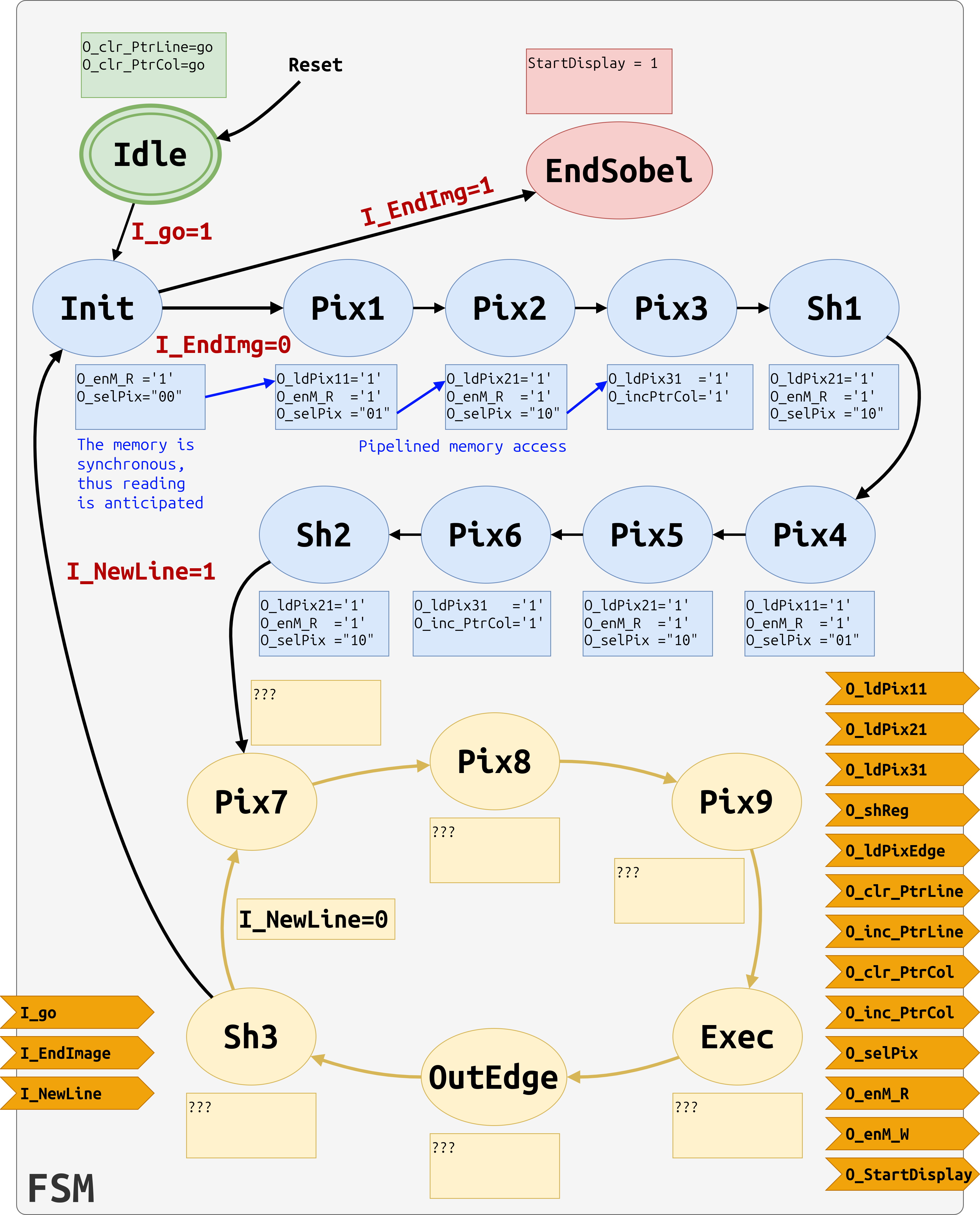
A skeleton of this FSM was presented in the introductory course with several signals already completed (see above). Thus, you are asked to work on the finalization (and possibly optimization) of this FSM.
Question 11: Complete the state machine diagram
This diagram is to be completed in order to then complete the VHDL file automate.vhd. To do this, you can use the file automate.drawio available in the git repository, it is the file docs/img/automate.drawio with the tool https://app.diagrams.net/. Then update the file automate.png by exporting the diagram automate.drawio previously updated.
Complete the automate.vhd file to model this FSM in VHDL.
Use the provided testbench (tb_automate.vhd) to validate the operation of the FSM by simulation. In the simulation, note the possibility of checking the evolution of the FSM states by displaying the enumerated type signal current_state.
Question 12: How many processes are used to describe the FSM, and what are their natures? Their sensitivity lists? Did the functional simulation validate the module? Justify
(answer to be completed in the file docs/compte-rendu.md)
Logic synthesis of the FSM⚓
Perform a logic synthesis and record the performance obtained in terms of resources used (Flip-Flops, LUTs, …) on the target FPGA considered.
Question 13: Give the results obtained
(answer to be completed in the file docs/compte-rendu.md)
Integration of the processor and prototyping⚓
Integration of the complete architecture of the Sobel processor⚓
To assemble the units that make up the Sobel processor, the VHDL module sobelProc.vhd was created and added to your project. This module instantiates the operative unit, the address generator, and the finite state machine.
Use the provided testbench (tb_sobelProc.vhd) to validate the operation of the processor by simulation.
Question 14: Did the functional simulation validate the module? Justify
(answer to be completed in the file docs/compte-rendu.md)
Perform a logic synthesis and record the performance obtained in terms of resources used (Flip-Flops, LUTs, …) on the target FPGA considered.
Question 15: Give and comment on the results obtained. What is the percentage of resources used by the Sobel processor compared to those available on the target Artix 7 FPGA XC7A100T-CSG324-1. Comment
(answer to be completed in the file docs/compte-rendu.md)
Prototyping and demonstration on board⚓
To finalize the validation of the designed processor, it must be integrated into a complete system with an input memory (test image), an output memory, and a display system.
For the test image, the famous Lena photo is made available with a resolution of 100x100 and an 8-bit gray level coding.
For the display system, we provide a VHDL-coded interface block to use the VGA controller integrated on the board.
The VHDL module sobelSys.vhd was created and added to your project. This module instantiates the Sobel processor, input and output memories, as well as the VGA controller. Check its structure and content.
Perform a logic synthesis and record the performance obtained in terms of resources used (Flip-Flops, LUTs, memories, …) on the target FPGA considered.
Question 16: Give and comment on the results obtained.
(answer to be completed in the file docs/compte-rendu.md)
For the final hardware compilation and prototyping on the board, a constraints file (Nexys4_Sobel.xdc) has been added to your project to route the input/output ports to the corresponding pins of the FPGA. In addition, an image has been added to be loaded into the input memory. This image has already been converted to 8-bit coded gray levels and placed in a text file in the correct format (dancing_spider.txt).
Go through the design flow to produce the bitstream. This is the FPGA configuration file that specifies how the FPGA will be used to provide the circuit designed in VHDL and constrained by the file that specifies the inputs/outputs.
Once the bitstream generation is complete, you can connect a Nexys 4 board and a VGA screen before transferring the bitstream to the FPGA of the board via the dedicated USB programming port.
Info
Depending on the current TP conditions, you may need to deposit the generated bitstream file (sobelSys.bit) on Moodle. The teacher will test it on the board. The generated bitstream is located in the subdirectory sobel/sobel.runs/impl_1.
Question 17: Is the prototyping and demonstration on the board conclusive?
(answer to be completed in the file docs/compte-rendu.md)
Performance analysis⚓
This final phase of the project is dedicated to performance analysis.
Some results have already been recorded from the synthesis reports generated by the design tool, others remain to be calculated or extrapolated analytically.
To identify the maximum clock frequency achievable on this FPGA of the designed system, we can analyze the Report timing summary report after routing as indicated in this screenshot:

In this report, look for the Max Delay Paths section and record the value of the Data Path Delay. This value corresponds to the minimum clock period, i.e. the delay of the critical path of the circuit. The critical path is also indicated (its source and destination are identified). The maximum clock frequency is the inverse of this minimum period!

Note that we use a clock frequency of 25 MHz on the board (i.e. a period of 40 ns), well below the maximum frequency. The system must therefore run correctly with this operating frequency.
Question 18: Identify the maximum clock frequency achievable on this FPGA
(answer to be completed in the file docs/compte-rendu.md)
Question 19: How many clock cycles are needed to process a pixel?
(answer to be completed in the file docs/compte-rendu.md)
Question 20: How many clock cycles are needed to process a 396x396 definition image
(answer to be completed in the file docs/compte-rendu.md)
Question 21: How many 396x396 definition images can this processor process per second?
(answer to be completed in the file docs/compte-rendu.md)
Bonus – to go further⚓
For those who manage to complete the project in advance and wish to go further, several ideas can be investigated to exploit other levels of parallelism and improve performance by reducing execution time. In addition to the possibility of duplicating the processor to design a multi-core architecture, other alternatives can be considered for the architecture of the operative unit. The following gives two examples of architectural variants of the register bank of the operative unit. Such architectures, however, imply corresponding changes in the rest of the components (functional units, FSM, and probably memory interfaces). You can possibly study, at least analytically, the performance achievable in terms of execution time with one of these different architectures.

And if other ideas for development or optimization come to mind, do not hesitate to propose and discuss them with the teaching team!